| Substrate: |
c-plane sapphire |
| Crystal Structure of AlN Epitaxial Layer: |
wurtzite |
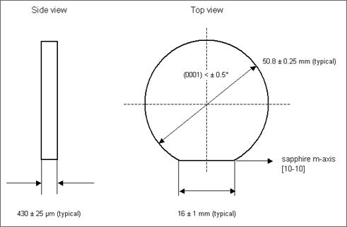
| Diameter: |
50.8 mm ± 0.25 mm (typical) |
| Thickness of Substrate: |
430 μm ± 25 μm (typical) |
| Thickness of AlN Epitaxial Layer: |
1 μm ± 0.3 μm (typical) |
| Surface: |
c-plane AlN, as grown effective area < 40 mmΦ (typical) no cracks by a visual inspection. |
| Backside: |
rough |
| FWHM of X-ray ω-scan rocking curve: |
< 150 arcsec for (0002) (typical) |
| Conductivity: |
insulating |
| Packing: |
packaged fluoroware container and vacuum-packed. |