
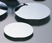
Gallium Arsenide Wafer
Our Gallium Arsenide Wafers are used in a wide range of fields including electronics devices such as laser applications for DVD, LED, and mobile phones.
| Applications |
| The wafers are used in high-output LDs, VCSEL, micro LEDs and display LEDs. |
 |
| Product features |
| VGF and LEC methods are used to develop single crystals. |
| The wafers are characterized by highly controlled carrier density and low EPD. |
| Product characteristics |
| VGF |
| VGF-n type, LD grade | VGF-n type, LED grade | ||||||||
| Crystal growth method | VGF (vertical gradient freezing) method | VGF (vertical gradient freezing) method | |||||||
| Dopant and conductive type | N type: Si-doped | N type: Si-doped | |||||||
| Carrier density | N-type (0.4-4)E18 cm-3 (Adjustable within the above range) |
N-type (0.4-4)E18 cm-3 (Adjustable within the above range) |
|||||||
| Dislocation density(EPD) | (cm-2) | EPDave≤200(LD) EPDmax≤2,000(LD) |
EPDave≤500(LED) EPDmax≤5,000(LED) |
||||||
| Size | 6-inch | 4-inch | 3-inch | 2-inch | 6-inch | 4-inch | 3-inch | 2-inch | |
| Plane orientation | 1. (100)0°~15°off±0.3 2. We will aim to meet your requests. |
1. (100)0°~15°off±0.3 2. We will aim to meet your requests. |
|||||||
| Diameter | (mm) | 150.0±0.3 | 100.0±0.3 | 76.0±0.3 76.2±0.3 |
50.0±0.3 50.8±0.3 |
150.0±0.3 | 100.0±0.3 | 76.0±0.3 76.2±0.3 |
50.0±0.3 50.8±0.3 |
| Thickness | (μm) | 625/675 ±25 |
450/625 ±25 |
350/450 ±25 |
350/450 ±25 |
625/675 ±25 |
450/625 ±25 |
350/450 ±25 |
350/450 ±25 |
| Orientation flat length | OF(mm) IF(mm) |
48.0±1.0 30.0±1.0 |
32.5±1.0 18.0±1.0 |
22.0±1.0 12.0±1.0 |
16.0±1.0 8.0±1.0 |
48.0±1.0 30.0±1.0 |
32.0±1.0 18.0±1.0 |
22.0±1.0 12.0±1.0 |
16.0±1.0 8.0±1.0 |
| (Adjustable upon request) | (Adjustable upon request) | ||||||||
| Orientation flat direction | OF Position IF Position |
EJ (Dove-Tail):[OF] (0-1-1)±0.05°/ [IF](0-11)±0.5° or SEMI US (V-Groove):[OF] (01-1)±0.05°/ [IF](011)±0.5° (Adaptable to both cleavage and bevel) |
EJ (Dove-Tail):[OF] (0-1-1)±0.5°/ [IF](0-11)±0.5° or SEMI US (V-Groove):[OF] (01-1)±0.5°/ [IF](011)±0.5° |
||||||
| Notch | OK | Not allowed | Not allowed | Not allowed | OK | Not allowed | Not allowed | Not allowed | |
| Edge rounding | Beveled | Beveled | |||||||
| Metalworking precision | TTV(μm) | ≤10.0 | ≤10.0 | ≤10.0 | ≤10.0(TV) | ≤10.0 | ≤10.0 | ≤10.0 | ≤10.0(TV) |
| Warp(μm) | ≤10.0 | ≤10.0 | ≤10.0 | ≤10.0 | ≤15.0 | ≤15.0 | ≤15.0 | ≤15.0 | |
| Surfacing | Surface | Mirror | Mirror | ||||||
| Back | Post-lap etching (mirror processing is also available) | Post-lap etching (mirror processing is also available) | |||||||
| Surface processing | Epi-ready | Epi-ready | |||||||
| Laser mark | Option | Option | |||||||
| Packaging form | Cassette | Cassette or individual packaging tray | Cassette | Cassette or individual packaging tray | |||||
|
VGF-p type
|
| VGF-p type Zn-doped | VGF-p type Zn- and Si-doped | ||||
| Carrier density | VGF (vertical gradient freezing) method | VGF (vertical gradient freezing) method | |||
| Dopant and conductive type | P type: Zn-doped | P type: Zn- and Si-doped | |||
| Carrier density | P-type (0.5-3)E19 cm-3 (Adjustable within the above range) |
P-type (0.5-3)E19 cm-3 (Adjustable within the above range) |
|||
| Dislocation density (EPD) | (cm-2) | EPDave</=3,000 EPDmax</=10,000 |
EPDave</=1,500 EPDmax</=10,000 |
||
| Size | 4-inch | 2-inch | 4-inch | 2-inch | |
| Plane orientation | 1. (100)0°/2°off±0.3 2. We will aim to meet your requests. |
1. (100)0°/2°off±0.3 2. We will aim to meet your requests. |
|||
| Diameter | (mm) | 100.0±0.3 | 50.0±0.3 50.8±0.3 |
100.0±0.3 | 50.0±0.3 50.8±0.3 |
| Thickness | (μm) | 450/625 ±25 |
350/450 ±25 |
450/625 ±25 |
350/450 ±25 |
| Orientation flat length | OF(mm) IF(mm) |
32.5±1.0 18.0±1.0 |
16.0±1.0 8.0±1.0 |
32.5±1.0 18.0±1.0 |
16.0±1.0 8.0±1.0 |
| (Adjustable upon request) | (Adjustable upon request) | ||||
| Orientation flat direction | OF(mm) IF(mm) |
EJ (Dove-Tail):[OF] (0-1-1)±0.05°/ [IF](0-11)±0.5° or SEMI US (V-Groove):[OF] (01-1)±0.05°/ [IF](011)±0.5° (Adaptable to both cleavage and bevel) |
EJ (Dove-Tail):[OF] (0-1-1)±0.05°/ [IF](0-11)±0.5° or SEMI US (V-Groove):[OF] (01-1)±0.05°/ [IF](011)±0.5° (Adaptable to both cleavage and bevel) |
||
| Edge rounding | Beveled | Beveled | |||
| Metalworking precision | TTV(μm) | ≤10.0 | ≤10.0(TV) | ≤10.0 | ≤10.0(TV) |
| Warp(μm) | ≤10.0 | ≤10.0 | ≤10.0 | ≤10.0 | |
| Surfacing | Surface | Mirror | Mirror | ||
| Back | Post-lap etching (mirror processing is also available) | Post-lap etching (mirror processing is also available) | |||
| Surface processing | Epi-ready | Epi-ready | |||
| Laser mark | Option | Option | |||
| Packaging form | Cassette or individual packaging tray | Cassette or individual packaging tray | |||
| Semi-insulating properties |
| VGF semi-insulating properties | LEC semi-insulating properties | ||||
| Carrier density | VGF (vertical gradient freezing) method | LEC (Liquid Encapsulated Czochralski) method | |||
| Dopant and conductive type | Semi-insulating properties: Undoped (C-doped) | Semi-insulating properties: Undoped (C-doped) | |||
| Resistivity | (at 22℃)(Ω cm) | ≧1E7 (Adjustable within the above range) |
≧1E7 (Adjustable within the above range) |
||
| Dislocation density (EPD) | (cm-2) | EPDave≤5000 | EPDave≤105 | ||
| Size | 4-inch | 3-inch | 4-inch | 3-inch | |
| Plane orientation | 1. (100)0°/2°off±0.3 2. We will aim to meet your requests. |
1. (100)0°/2°off±0.3 2. We will aim to meet your requests. |
|||
| Diameter | (mm) | 100.0±0.3 | 76.0±0.3 76.2±0.3 |
100.0±0.3 | 76.0±0.3 76.2±0.3 |
| Thickness | (μm) | 450/625 ±25 |
350/450 ±25 |
450/625 ±25 |
350/450 ±25 |
| Orientation flat length | OF(mm) IF(mm) |
32.5±1.0 18.0±1.0 |
22.0±1.0 12.0±1.0 |
32.5±1.0 18.0±1.0 |
22.0±1.0 12.0±1.0 |
| (Adjustable upon request) | (Adjustable upon request) | ||||
| Orientation flat direction | OF Position IF Position |
EJ (Dove-Tail):[OF] (0-1-1)±0.5°/ [IF](0-11)±0.5° or SEMI US (V-Groove):[OF] (01-1)±0.5°/ [IF](011)±0.5° |
EJ (Dove-Tail):[OF] (0-1-1)±0.5°/ [IF](0-11)±0.5° or SEMI US (V-Groove):[OF] (01-1)±0.5°/ [IF](011)±0.5° |
||
| Edge rounding | Beveled | Beveled | |||
| Metalworking precision | TTV(μm) | ≤10.0 | ≤10.0 | ≤10.0 | ≤10.0 |
| Metalworking precision | TIR(μm) | ≤5.0 | ≤5.0 | ≤5.0 | ≤5.0 |
| Metalworking precision | Warp(μm) | ≤10.0 | ≤10.0 | ≤10.0 | ≤10.0 |
| Surfacing | Surface | Mirror | Mirror | ||
| Back | Post-lap etching (mirror processing is also available) | Post-lap etching (mirror processing is also available) | |||
| Surface processing | Epi-ready | Epi-ready | |||
| Laser mark | Option | Option | |||
| Packaging form | Cassette or individual packaging tray | Cassette or individual packaging tray | |||