
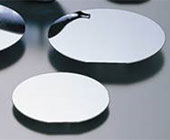
砷化镓基板
本公司的砷化镓基板大量应用于DVD等激光设备以及LED、手机等电子设备,用途广泛。
| 用途 |
| 应用于大功率LD、VCSEL、Micro LED及显示屏LED基板。 |
 |
| 产品特点 |
| 通过VGF法和LEC法培养单晶。 |
| 拥有高度控制载流子浓度、低EPD等特点。 |
| 产品特性 |
| VGF |
| VGF-n 型, LD grade | VGF-n 型, LED grade | ||||||||
| Crystal growth method | VGF (vertical gradient freezing) method | VGF (vertical gradient freezing) method | |||||||
| Dopant and conductive type | N type: Si-doped | N type: Si-doped | |||||||
| Carrier density | N-type (0.4-4)E18 cm-3 (Adjustable within the above range) |
N-type (0.4-4)E18 cm-3 (Adjustable within the above range) |
|||||||
| Dislocation density(EPD) | (cm-2) | EPDave≤200(LD) EPDmax≤2,000(LD) |
EPDave≤500(LED) EPDmax≤5,000(LED) |
||||||
| Size | 6-inch | 4-inch | 3-inch | 2-inch | 6-inch | 4-inch | 3-inch | 2-inch | |
| Plane orientation | 1. (100)0 °~15 °off±0.3 2. We will aim to meet your requests. |
1. (100)0 °~15 °off±0.3 2. We will aim to meet your requests. |
|||||||
| Diameter | (mm) | 150.0±0.3 | 100.0±0.3 | 76.0±0.3 76.2±0.3 |
50.0±0.3 50.8±0.3 |
150.0±0.3 | 100.0±0.3 | 76.0±0.3 76.2±0.3 |
50.0±0.3 50.8±0.3 |
| Thickness | (μm) | 625/675 ±25 |
450/625 ±25 |
350/450 ±25 |
350/450 ±25 |
625/675 ±25 |
450/625 ±25 |
350/450 ±25 |
350/450 ±25 |
| Orientation flat length | OF(mm) IF(mm) |
48.0±1.0 30.0±1.0 |
32.5±1.0 18.0±1.0 |
22.0±1.0 12.0±1.0 |
16.0±1.0 8.0±1.0 |
48.0±1.0 30.0±1.0 |
32.0±1.0 18.0±1.0 |
22.0±1.0 12.0±1.0 |
16.0±1.0 8.0±1.0 |
| (Adjustable upon request) | (Adjustable upon request) | ||||||||
| Orientation flat direction | OF Position IF Position |
EJ (Dove-Tail):[OF] (0-1-1)±0.05 °/ [IF](0-11)±0.5 ° or SEMI US (V-Groove):[OF] (01-1)±0.05 °/ [IF](011)±0.5 ° (Adaptable to both cleavage and bevel) |
EJ (Dove-Tail):[OF] (0-1-1)±0.5 °/ [IF](0-11)±0.5 ° or SEMI US (V-Groove):[OF] (01-1)±0.5 °/ [IF](011)±0.5 ° |
||||||
| Notch | OK | Not allowed | Not allowed | Not allowed | OK | Not allowed | Not allowed | Not allowed | |
| Edge rounding | Beveled | Beveled | |||||||
| Metalworking precision | TTV(μm) | ≤10.0 | ≤10.0 | ≤10.0 | ≤10.0(TV) | ≤10.0 | ≤10.0 | ≤10.0 | ≤10.0(TV) |
| Metalworking precision | Warp(μm) | ≤10.0 | ≤10.0 | ≤10.0 | ≤10.0 | ≤15.0 | ≤15.0 | ≤15.0 | ≤15.0 |
| Surfacing | Surface | Mirror | Mirror | ||||||
| Surfacing | Back | Post-lap etching (mirror processing is also available) | Post-lap etching (mirror processing is also available) | ||||||
| Surface processing | Epi-ready | Epi-ready | |||||||
| Laser mark | Option | Option | |||||||
| Packaging form | Cassette | Cassette or individual packaging tray | Cassette | Cassette or individual packaging tray | |||||
|
VGF-p型
|
| VGF-p型 Zn-doped | VGF-p型 Zn- and Si-doped | ||||
| Carrier density | VGF (vertical gradient freezing) method | VGF (vertical gradient freezing) method | |||
| Dopant and conductive type | P type: Zn-doped | P type: Zn- and Si-doped | |||
| Carrier density | P-type (0.5-3)E19 cm-3 (Adjustable within the above range) |
P-type (0.5-3)E19 cm-3 (Adjustable within the above range) |
|||
| Dislocation density (EPD) | (cm-2) | EPDave</=3,000 EPDmax</=10,000 |
EPDave</=1,500 EPDmax</=10,000 |
||
| Size | 4-inch | 2-inch | 4-inch | 2-inch | |
| Plane orientation | 1. (100)0 °/2 °off±0.3 2. We will aim to meet your requests. |
1. (100)0 °/2 °off±0.3 2. We will aim to meet your requests. |
|||
| Diameter | (mm) | 100.0±0.3 | 50.0±0.3 50.8±0.3 |
100.0±0.3 | 50.0±0.3 50.8±0.3 |
| Thickness | (μm) | 450/625 ±25 |
350/450 ±25 |
450/625 ±25 |
350/450 ±25 |
| Orientation flat length | OF(mm) IF(mm) |
32.5±1.0 18.0±1.0 |
16.0±1.0 8.0±1.0 |
32.5±1.0 18.0±1.0 |
16.0±1.0 8.0±1.0 |
| (Adjustable upon request) | (Adjustable upon request) | ||||
| Orientation flat direction | OF(mm) IF(mm) |
EJ (Dove-Tail):[OF] (0-1-1)±0.05 °/ [IF](0-11)±0.5 ° or SEMI US (V-Groove):[OF] (01-1)±0.05 °/ [IF](011)±0.5 ° (Adaptable to both cleavage and bevel) |
EJ (Dove-Tail):[OF] (0-1-1)±0.05 °/ [IF](0-11)±0.5 ° or SEMI US (V-Groove):[OF] (01-1)±0.05 °/ [IF](011)±0.5 ° (Adaptable to both cleavage and bevel) |
||
| Edge rounding | Beveled | Beveled | |||
| Metalworking precision | TTV(μm) | ≤10.0 | ≤10.0(TV) | ≤10.0 | ≤10.0(TV) |
| Warp(μm) | ≤10.0 | ≤10.0 | ≤10.0 | ≤10.0 | |
| Surfacing | Surface | Mirror | Mirror | ||
| Back | Post-lap etching (mirror processing is also available) | Post-lap etching (mirror processing is also available) | |||
| Surface processing | Epi-ready | Epi-ready | |||
| Laser mark | Option | Option | |||
| Packaging form | Cassette or individual packaging tray | Cassette or individual packaging tray | |||
| 半绝缘性能 |
| VGF 半绝缘性能 | LEC 半绝缘性能 | ||||
| Carrier density | VGF (vertical gradient freezing) method | LEC (Liquid Encapsulated Czochralski) method | |||
| Dopant and conductive type | 半绝缘性能: Undoped (C-doped) | 半绝缘性能: Undoped (C-doped) | |||
| Resistivity | (at 22℃)(Ω cm) | ≧1E7 (Adjustable within the above range) |
≧1E7 (Adjustable within the above range) |
||
| Dislocation density (EPD) | (cm-2) | EPDave≤5000 | EPDave≤10^5 | ||
| Size | 4-inch | 3-inch | 4-inch | 3-inch | |
| Plane orientation | 1. (100)0 °/2 °off±0.3 2. We will aim to meet your requests. |
1. (100)0 °/2 °off±0.3 2. We will aim to meet your requests. |
|||
| Diameter | (mm) | 100.0±0.3 | 76.0±0.3 76.2±0.3 |
100.0±0.3 | 76.0±0.3 76.2±0.3 |
| Thickness | (μm) | 450/625 ±25 |
350/450 ±25 |
450/625 ±25 |
350/450 ±25 |
| Orientation flat length | OF(mm) IF(mm) |
32.5±1.0 18.0±1.0 |
22.0±1.0 12.0±1.0 |
32.5±1.0 18.0±1.0 |
22.0±1.0 12.0±1.0 |
| (Adjustable upon request) | (Adjustable upon request) | ||||
| Orientation flat direction | OF Position IF Position |
EJ (Dove-Tail):[OF] (0-1-1)±0.5 °/ [IF](0-11)±0.5 ° or SEMI US (V-Groove):[OF] (01-1)±0.5 °/ [IF](011)±0.5 ° |
EJ (Dove-Tail):[OF] (0-1-1)±0.5 °/ [IF](0-11)±0.5 ° or SEMI US (V-Groove):[OF] (01-1)±0.5 °/ [IF](011)±0.5 ° |
||
| Edge rounding | Beveled | Beveled | |||
| Metalworking precision | TTV(μm) | ≤10.0 | ≤10.0 | ≤10.0 | ≤10.0 |
| TIR(μm) | ≤5.0 | ≤5.0 | ≤5.0 | ≤5.0 | |
| Warp(μm) | ≤10.0 | ≤10.0 | ≤10.0 | ≤10.0 | |
| Surfacing | Surface | Mirror | Mirror | ||
| Back | Post-lap etching (mirror processing is also available) | Post-lap etching (mirror processing is also available) | |||
| Surface processing | Epi-ready | Epi-ready | |||
| Laser mark | Option | Option | |||
| Packaging form | Cassette or individual packaging tray | Cassette or individual packaging tray | |||